- 您现在的位置:买卖IC网 > Sheet目录320 > DK-DEV-2AGX260N (Altera)KIT DEV FPGA 2AGX260 W/6.375G TX
�� �
�
�A.� Programming� the� Flash� Memory�
�Device�
�Introduction�
�As� you� develop� your� own� project� using� the� Altera� tools,� you� can� program� the� flash�
�memory� device� so� that� your� own� design� loads� from� flash� memory� into� the� FPGA� on�
�power� up.� This� appendix� describes� the� preprogrammed� contents� of� the� common� flash�
�interface� (CFI)� flash� memory� device� on� the� Arria� II� GX� FPGA� development� board,� 6G�
�edition� and� the� Nios� II� EDS� tools� involved� with� reprogramming� the� user� portions� of�
�the� flash� memory� device.�
�The� Arria� II� GX� FPGA� development� board,� 6G� edition� ships� with� the� CFI� flash� device�
�preprogrammed� with� a� default� factory� FPGA� configuration� for� running� the� Board�
�Update� Portal� design� example� and� a� default� user� configuration� for� running� the� Board�
�Test� System� demonstration.� There� are� several� other� factory� software� files� written� to�
�the� CFI� flash� device� to� support� the� Board� Update� Portal.� These� software� files� were�
�created� using� the� Nios� II� EDS,� just� as� the� hardware� design� was� created� using� the�
�Quartus� II� software.�
��page� of� the� Altera� website.�
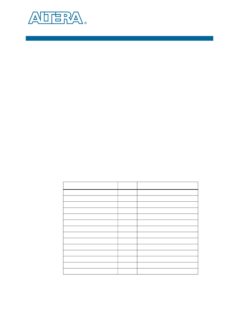
�CFI� Flash� Memory� Map�
�Table� A–1� shows� the� default� memory� contents� of� the� 512-Mb� (64-MB)� single-die� CFI�
�flash� device.� For� the� Board� Update� Portal� to� run� correctly� and� update� designs� in� the�
�user� memory,� this� memory� map� must� not� be� altered.�
�Table� A–1.� Byte� Address� Flash� Memory� Map�
�Block� Description�
�Unused�
�Unused�
�Unused�
�Unused�
�User� software�
�Factory� software�
�zipfs� (html,� web� content)�
�User� hardware� 2�
�User� hardware� 1�
�Factory� hardware�
�PFL� option� bits�
�Board� information�
�Ethernet� option� bits�
�User� design� reset� vector�
�July� 2010� Altera� Corporation�
�Size�
�32� KB�
�32� KB�
�32� KB�
�32� KB�
�16,384� KB�
�8,1092� KB�
�8,192� KB�
�10,880� KB�
�10,880� KB�
�10,880� KB�
�32� KB�
�32� KB�
�32� KB�
�32� KB�
�Address� Range�
�0x03FF8000� -� 0x03FFFFFF�
�0x03FF0000� -� 0x03FF7FFF�
�0x03FE8000� -� 0x03FEFFFF�
�0x03FE0000� -� 0x03FE7FFF�
�0x0300.0000� -� 0x03FDFFFF�
�0x02800000� -� 0x02FFFFFF�
�0x02000000� -� 0x027FFFFF�
�0x01560000� -� 0x01FFFFFF�
�0x00AC0000� -� 0x0155FFFF�
�0x00020000� -� 0x00ABFFFF�
�0x00018000� -� 0x0001FFFF�
�0x00010000� -� 0x00017FFF�
�0x00008000� -� 0x0000FFFF�
�0x00000000� -� 0x00007FFF�
�Arria� II� GX� FPGA� Development� Kit,� 6G� Edition� User� Guide�
�发布紧急采购,3分钟左右您将得到回复。
相关PDF资料
DK-DEV-4SE530N
KIT DEV STRATIX IV FPGA 4SE530
DK-DEV-4SGX530N
KIT DEVELOPMENT STRATIX IV
DK-DEV-5AGXB3N/ES
ARRIA V DEVELOPMENT KIT
DK-DEV-5M570ZN
KIT DEV MAX V 5M570Z
DK-DEV-5SGXEA7N
KIT DEV STRATIX V FPGA 5SGXEA7
DK-DSP-2S180N
DSP PRO KIT W/SII EP2S180N
DK-DSP-3C120N
KIT DEV DSP CYCLONE III EDITION
DK-K7-CONN-CES-G
KINTEX-7 FPGA CONNECTIVITY KIT
相关代理商/技术参数
DK-DEV-3C120N
功能描述:可编程逻辑 IC 开发工具 FPGA Development Kit For EP3C120F780
RoHS:否 制造商:Altera Corporation 产品:Development Kits 类型:FPGA 工具用于评估:5CEFA7F3 接口类型: 工作电源电压:
DK-DEV-3CLS200N
功能描述:可编程逻辑 IC 开发工具 FPGA Development Kit For EP3CLS200F780
RoHS:否 制造商:Altera Corporation 产品:Development Kits 类型:FPGA 工具用于评估:5CEFA7F3 接口类型: 工作电源电压:
DK-DEV-3SL150N
功能描述:可编程逻辑 IC 开发工具 FPGA Development Kit For EP3SL150F152
RoHS:否 制造商:Altera Corporation 产品:Development Kits 类型:FPGA 工具用于评估:5CEFA7F3 接口类型: 工作电源电压:
DK-DEV-3SL150N/ES
制造商:Altera Corporation 功能描述:KIT DEVELOPMENT STRATIX II ES
DK-DEV-4CGX150N
功能描述:可编程逻辑 IC 开发工具 FPGA Development Kit For EP4CGX150
RoHS:否 制造商:Altera Corporation 产品:Development Kits 类型:FPGA 工具用于评估:5CEFA7F3 接口类型: 工作电源电压:
DK-DEV-4CGX150N
制造商:Altera Corporation 功能描述:KIT STARTER CYCLONE IV GX ((NS
DK-DEV-4S100G5N
功能描述:可编程逻辑 IC 开发工具 FPGA Development Kit For EP4S100G5F
RoHS:否 制造商:Altera Corporation 产品:Development Kits 类型:FPGA 工具用于评估:5CEFA7F3 接口类型: 工作电源电压:
DK-DEV-4SE530N
功能描述:可编程逻辑 IC 开发工具 FPGA Development Kit For EP4SE530H35
RoHS:否 制造商:Altera Corporation 产品:Development Kits 类型:FPGA 工具用于评估:5CEFA7F3 接口类型: 工作电源电压: